新書推薦:

《
论断与概念
》
售價:HK$
96.8

《
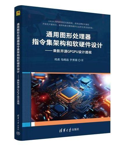
通用图形处理器指令集架构和软硬件设计——乘影开源GPGPU设计透视
》
售價:HK$
141.9

《
游牧者的抉择:面对汉帝国的北亚游牧部族
》
售價:HK$
76.8

《
从“四夷”到“外国”:《宋史·外国传》研究 国家社科基金后期资助项目
》
售價:HK$
96.8

《
苏格拉底的虔敬:读柏拉图《游叙弗伦》笔记
》
售價:HK$
86.9

《
思辨者的罗盘:从逻辑谬误到严谨表达
》
售價:HK$
61.6

《
面具之下:近代日本报人对华情报活动
》
售價:HK$
96.8

《
广东省博物馆藏品大系 端砚卷
》
售價:HK$
547.8
|
| 內容簡介: |
|
本书是一本介绍半导体集成电路和器件制造技术的专业书籍,在半导体领域享有很高的声誉。本书的范围包括半导体工艺的每个阶段:从原材料的制备到封装、测试和成品运输,以及传统的和现代的工艺。全书提供了详细的插图和实例,每章包含回顾总结和习题,并辅以丰富的术语表。第六版修订了微芯片制造领域的新进展,讨论了用于图形化、掺杂和薄膜步骤的先进工艺和尖端技术,使隐含在复杂的现代半导体制造材料和工艺中的物理、化学和电子的基础知识更易理解。本书的主要特点是避开了复杂的数学问题介绍工艺技术内容;加入了半导体业界的新成果,可以使读者了解工艺技术发展的趋势。
|
| 目錄:
|
Contents
1The Semiconductor Industry1
Introduction1
Birth of an Industry1
The Solid-State Era3
Integrated Circuits ICs4
Process and Product Trends5
Moore’s Law6
Decreasing Feature Size6
Increasing Chip and Wafer Size8
Reduction in Defect Density9
Increase in Interconnection Levels 10
The Semiconductor Industry Association Roadmap 10
Chip Cost 11
Industry Organization 11
Stages of Manufacturing 12
Six Decades of Advances in Microchip Fabrication Processes 14
The Nano Era 16
Review Topics 17
References 17
2Properties of Semiconductor Materials and Chemicals19
Introduction 19
Atomic Structure 19
The Bohr Atom 19
The Periodic Table of the Elements 20
Electrical Conduction 23
Conductors 23
Dielectrics and Capacitors 23
Resistors 24
Intrinsic Semiconductors 24
Doped Semiconductors 25
Electron and Hole Conduction 26
Carrier Mobility 28
Semiconductor Production Materials 29
Germanium and Silicon 29
Semiconducting Compounds 29
Silicon Germanium 31
Engineered Substrates 31
Ferroelectric Materials 31
Diamond Semiconductors 32
Process Chemicals 32
Molecules, Compounds, and Mixtures 32
Ions 33
States of Matter 34
Solids, Liquids, and Gases 34
Plasma State 34
Properties of Matter 34
Temperature 34
Density, Specic Gravity, and Vapor Density 35
Pressure and Vacuum 36
Acids, Alkalis, and Solvents 37
Acids and Alkalis 37
Solvents 38
Chemical Purity and Cleanliness 38
Safety Issues 38
The Material Safety Data Sheet 39
Review Topics 39
References 39
3Crystal Growth and Silicon Wafer Preparation 41
Introduction 41
Semiconductor Silicon Preparation 41
Silicon Wafer Preparation Stages 42
Crystalline Materials 42
Unit Cells 43
Poly and Single Crystals 43
Crystal Orientation 44
Crystal Growth 45
Czochralski Method 45
Liquid-Encapsulated Czochralski 47
Float Zone 47
Crystal and Wafer Quality 49
Point Defects 49
Dislocations 50
Growth Defects 50
Wafer Preparation 51
End Cropping 51
Diameter Grinding 51
Crystal Orientation, Conductivity, and Resistivity Check 51
Grinding Orientation Indicators 52
Wafer Slicing 53
Wafer Marking 54
Rough Polish 54
Chemical Mechanical Polishing 55
Backside Processing 55
Double-Sided Polishing 56
Edge Grinding and Polishing 56
Wafer Evaluation 56
Oxidation 57
Packaging 57
Wafer Types and Uses 57
Reclaim Wafers 57
Engineered Wafers Substrates 57
Review Topics 58
References 58
4Overview of Wafer Fabrication and Packaging 59
Introduction 59
Goal of Wafer Fabrication 59
Wafer Terminology 59
Chip Terminology 61
Basic Wafer-Fabrication Operations 63
Layering 63
Patterning 64
Circuit Design 66
Reticle and Masks 68
Doping 69
Heat Treatments 69
Example Fabrication Process 72
Wafer Sort 74
Packaging 75
Summary 75
Review Topics 76
References 76
5Contamination Control 77
Introduction 77
The Problem 77
Contamination-Caused Problems 80
Contamination Sources 81
General Sources 81
Air 81
Clean Air Strategies 82
Cleanroom Workstation Strategy 83
Tunnel or Bay Concept 85
Micro- and Mini-Environments 86
Temperature, Humidity, and Smog 87
Cleanroom Construction 88
Construction Materials 88
Cleanroom Elements 89
Personnel-Generated Contamination 93
Process Water 94
Process Chemicals 96
Equipment 99
Cleanroom Materials and Supplies 99
Cleanroom Maintenance 100
Wafer-Surface Cleaning 100
Particulate Removal 102
Wafer Scrubbers 102
High-Pressure Water Cleaning 103
Organic Residues 103
Inorganic Residues 103
Chemical-Cleaning Solutions 104
General Chemical Cleaning 104
Oxide Layer Removal 105
Room Temperature and Ozonated Chemistries 106
Water Rinsing 108
Drying Techniques 110
Contamination Detection 112
Review Topics 112
References 113
6Productivity and Process Yields 115
Overview 115
Yield Measurement Points 115
Accumulative Wafer-Fabrication Yield 116
Wafer-Fabrication Yield Limiters 117
Number of Process Steps 118
Wafer Breakage and Warping 118
Process Variation 119
Mask Defects 120
Wafer-Sort Yield Factors 120
Wafer Diameter and Edge Die 121
Wafer Diameter and Die Size 122
Wafer Diameter and Crystal Defects 122
Wafer Diameter and Process Variations 123
Die Area and Defect Density 124
Circuit Density and Defect Density 125
Number of Process Steps 125
Feature Size and Defect Size 125
Process Cycle Time 125
Wafer-Sort Yield Formulas 125
Assembly and Final Test Yields 128
Overall Process Yields 128
Review Topics 129
References 130
7Oxidation 131
Introduction 131
Silicon Dioxide Layer Uses 131
Surface Passivation 131
Doping Barrier 132
Surface Dielectric 132
Device Dielectric MOS Gates 133
Device Oxide Thicknesses 134
Thermal Oxidation Mechanisms 134
Influences on the Oxidation Rate137
Thermal Oxidation Methods140
Horizontal Tube Furnaces140
Temperature Control System141
Source Cabinet143
Vertical Tube Furnaces143
Rapid Thermal Processing146
High-Pressure Oxidation149
Oxidant Sources151
Oxidation Processes 154
Preoxidation Wafer Cleaning 154
Postoxidation Evaluation155
Surface Inspection156
Oxide Thickness156
Oxide and Furnace Cleanliness 156
Thermal Nitridation 156
Review Topics157
References157
8The Ten-Step Patterning Process—Surface Preparation to Exposure 161
Introduction161
Overview of the Photomasking Process 162
Ten-Step Process165
Basic Photoresist Chemistry167
Photoresist167
Photoresist Performance Factors169
Resolution Capability169
Adhesion Capability 170
Process Latitude171
Pinholes172
Particle and Contamination Levels173
Step Coverage173
Thermal Flow173
Comparison of Positive and Negative Resists173
Physical Properties of Photoresists175
Solids Content175
Viscosity 175
Surface Tension176
Index of Refraction 176
Storage and Control of Photoresists176
Light and Heat Sensitivity176
Viscosity Sensitivity177
Shelf Life177
Cleanliness177
Photomasking Processes—Surface Preparation to Exposure178
Surface Preparation 178
Particle Removal178
Dehydration Baking 178
Wafer Priming179
Spin Priming180
Vapor Priming180
Photoresist Application Spinning181
The Static Dispense Spin Process181
Dynamic Dispense183
Moving-Arm Dispensing183
Manual Spinners183
Automatic Spinners184
Edge Bead Removal185
Backside Coating185
Soft Bake 185
Convection Ovens186
Manual Hot Plates187
In-Line, Single-Wafer Hot Plates187
Moving-Belt Hot Plates187
Moving-Belt Infrared Ovens188
Microwave Baking188
Vacuum Baking188
Alignment and Exposure189
Alignment and Exposure Systems189
Exposure Sources191
Alignment Criteria191
Aligner Types193
Postexposure Bake196
Advanced Lithography198
Review Topics198
References198
9The Ten-Step Patterning Process—Developing to Final Inspection201
Introduction201
Development201
Positive Resist Development201
Negative Resist Development203
Wet Development Processes203
Dry or Plasma Development206
Hard Bake 207
Hard-Bake Methods207
Hard-Bake
|
|


